Instructions on FPGA Board and Xilinx software
Prepared by
Diego Campos (SPRING 2002): 1.0,1.5,2.0
Updated by
Matthew Klepeis (SPRING 2003): 3.0
Snehesh Shrestha (SPRING 2004): 4.0
Steve Sanko (SPRING 2005): 4.1
Brian Moran (SPRING 2006): 4.2
Version 4.2
Last update –3/14/06
Edited by Dr. Joseph Wunderlich
I.
XILINX AND FPGA INTRODUCTION
Field-Programmable Gate Array (FPGA) - A logic chip which can be programmed to function as an array of computational logic blocks.
Xilinx Software - Xilinx Software allows a designer to graphically create a logic circuit which can be tested and simulated prior to implementation on the FPGA board.
FPGA vs Breadboarding [1]
• FPGA’s simplify design, implementation, testing, and debugging
• Reusable - Easily reprogrammed and reconfigured
• Most are non volatile
• Useful in prototyping IC designs
• Low power
• High number of gates/parts in the same area
• HDL helps create libraries (new gates or parts) and functional blocks
• Do not need to worry about voltage, current, or power to each gate or circuit part
• Circuit can be simulated and debugged before implementation; therefore saving time and money
FPGAs can be programmed using schematics to lay out a design, or by using an HDL like Verilog or VHDL. Our Xilinx software license only allows schematic design. As well as being cheap to program for an application, FPGA hardware is cheap as well. A Spartan 3E costs from $2-$9 (March 2006), depending on the number of gates possible, the number of pins, and the size of the order. Some FPGAs include a von Neumann architecture processor on the same die as the FPGA, usually with a clock speed of under 1GHz. Xilinx has a 450MHz PowerPC processor embedded in its Virtex-4 design, and Actel’s Fusion design is available with an ARM7 processor. FPGAs can be used for complex applications, such as image processing or image compression, and are suitable for use in portable phones, digital cameras, and other complex digital applications. Xilinx, as well as other companies sell intellectual property (IP) cores, and opencores.org provides cores and source code for free under the GPL.
Evaluating the performance of an FPGA is difficult. Most manufacturers don’t provide a gate count for their products, because it tends to be misleading. Mostly, FPGA manufacturers give a number of “logic units” or “logic cells,” which consist of a lookup table and a flip-flop, as well as assorted connection logic. Because different manufacturers use different types of basic gates (AND vs. NAND, etc), the gate count of a logic unit isn’t the same across different manufacturers, or even different FPGAs. Currently, the high-end Virtex-4 designs have 200,000 logic cells, the midrange Spartan 3E design has from 2-33,000 logic cells, the Spartan FPGA used in lab has 466 logic cells.
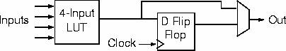
A logic block of an FPGA
FPGAs are becoming more sophisticated, and their applications are expanding as they become more capable. Currently, Cray uses Xilinx FPGAs in their XD1 supercomputer. When doing calculations that can be made in parallel, the FPGAs are programmed to deal specifically with this problem. Because of the high speed I/O capabilities of the FPGA, it is ideal for acceleration of certain problems. This is an emerging area of FPGA use, and is still in the research stages.
II. INSTALLING SOFTWARE
While we use Xilinx Foundation 4 in lab, Xilinx has changed their development to ISE Foundation, which has enhanced capabilities for place-and-route, as well as more robust verification, timing, and planning tools. A free development system is available from Xilinx. ISE WebPack, is currently at version 8.1i, and is available for Windows and Linux. While the WebPack does not support the Spartan FPGA used in our development boards, it does support the Spartan 3E. Spartan 3E development boards are available from Xilinx for around $150 (March 2006).
The Computer Organization book comes with Xilinx ISE Student Edition 4.1i. This version is incompatible with Windows XP, and does not support our FPGA; however it can be used to create schematics and HDL designs and simulate them, so if programming an FPGA board isn’t required this software is suitable.
a. Begin by inserting CD labeled Program files, not Documentation.
b. Serial Key # is as follows for the 4.1 version of Xilinx software:
0215-0455-9922
c. When prompted, select to install Spartan chip drivers. Select any other chip driver specified by Instructor (FPGA labs using testing board uses Spartan). Do not deselect any default, continue with installation.
d. When prompted, select to install Parallel Cable III driver. This will allow download from computer to board. DO NOT SKIP THIS STEP!
e. Installation may last anywhere from 15-20 minutes. It will take a while, do not stop installation unless time limit has gone above 30 minutes and installation bar has not moved. If you receive an error during installation, software may work. Whether you wish to repeat installation process is, of course, limited with the restrain of how much time you have to work on the labs. INSTALL SOFTWARE AND TEST IT AT A MINIMUM OF A WEEK IN ADVANCE. THIS WILL SAVE THE INSTRUCTOR AND YOUR COLLEAGUES THE TIME TO INSTALL IT. FURTHER GRADES WILL ASSUME THAT STUDENTS KNOW HOW TO INSTALL THIS ON THEIR COMPUTERS. THIS IS ALSO ASSUMING THAT A STUDENT MAY WISH TO INSTALL THE SOFTWARE ON THEIR OWN COMPUTER. THE VERSION USED IN LAB IS DIFFERENT AND THE CODES ARE DIFFERENT. INSTALL AND USE AT YOUR OWN EXPENSE, REALIZE CODE MAY NOT WORK, AND DOWNLOADS MAY NOT WORK DUE TO LICENSE.
f. After installing the FPGA Express, the Foundation software will start to install. This is the program manager required to make schematics that can be downloaded to the testing board. Follow any steps necessary and continue until the computer prompts to restart.
g. After installation is complete, do not restart the computer, if given a choice. If the computer can only restart after installation, go to step h. Else, go to the black disk that is included in the installation package for the FPGA software. Go to the directory c:\Xilinx\data\ and replace the file called license.dat with the one on the disk. After doing so, go to the c:\ directory and edit the autoexec.bat file. Insert the following line of text to be booted at startup:
set LM_LICENSE_FILE=<path_to_license>\license.dat
Of course, <path_to_license> in this example was c:\Xilinx\data\ . Add the line after any lines booting vital hardware (e.g. sound, etc.) Skip step h.
h. Add
the line of text of
SET LM_LICENSE_FILE=<path_to_license>\license.dat
to the autoexec.bat
file on the c:\ directory. Where <path_to_license> is determined by where the license file
was placed by the software (merely do a Find license.dat
on c:\ ).
i.
Reboot.
j.
To make
sure the program works, go to the autoexec.bat file and edit it. Before doing so, look in the My Computer and
check the drive letter for the CD_ROM drive, you’ll need it since the letter
isn’t universal. Make sure the following
lines of code are in the bat file or Xilinx will not compile your schematic
to machine code on the Implementation part of the download to the FPGA:
SET
XILINX_CD=CD_DRIVE_LETTER:
SET XILINX=C:\XILINX
SET
PATH=C:\XILINX\BIN\NT;C:\FNDTN\BIN\NT;
The previous line of code
should be followed by the code C:\WINDOWS;C:\WINDOWS\COMMAND
The bat file should already contain such a line of code, merely append it so that the other path lines appear prior. The other lines of code should go towards the end of the bat file.
III.
USING XILINX FOUNDATION SERIES
a. Start program called “Xilinx Foundation
Project Manager. This may not be on
desktop but under the Programs folder in the Start Menu.
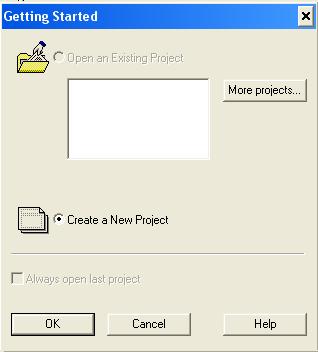
b. Create a new project.
c. Name the project and select Spartan
for the chipset below the world “Flow:” on the control box.
d. Make sure you select the chip specification
to be S10PC84.
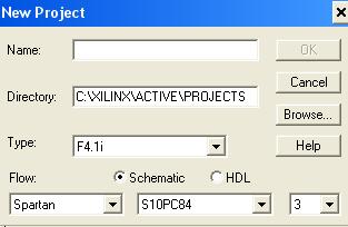
e. Leave all other defaults and click okay,
unless instructor specifies a different file folder to save files.
f.
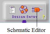
Select the
Schematic Editor which is third on right icon.
g. Once the grid appears you must select parts
for your schematic. Most of the time,
you will be using the “Draw Wires” and “Symbols Toolbox”.
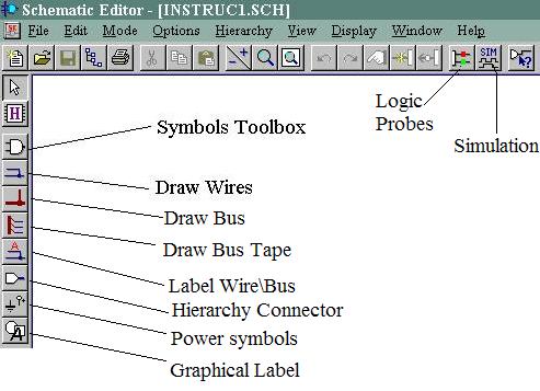
![]() Activates
select and drag mode. This mode allows you to:
Activates
select and drag mode. This mode allows you to:
· Select Schematic objects for various operations
· Move Schematic objects using the drag and drop methodology
![]() Activates
the hierarchy mode. This mode allows you to descend into a hierarchal macro and
view its contents.
Activates
the hierarchy mode. This mode allows you to descend into a hierarchal macro and
view its contents.
![]() Activates
the symbol mode. This mode allows you to select parts for placement in the
schematic.
Activates
the symbol mode. This mode allows you to select parts for placement in the
schematic.
![]() Activates
the draw wires mode. This mode allows you to draw electrical connections
between circuit components.
Activates
the draw wires mode. This mode allows you to draw electrical connections
between circuit components.
![]() Activates
the draw busses mode. This mode allows you to draw busses.
Activates
the draw busses mode. This mode allows you to draw busses.
![]() Activates
the draw bus taps mode. This mode allows
you to place bus taps which are transitions between a bus and a discrete wire.
Activates
the draw bus taps mode. This mode allows
you to place bus taps which are transitions between a bus and a discrete wire.
![]() Activates
the Add Net Name window. This enables you to add a label to an existing wire or
bus. Names are linked via wires in the same manner as other circuit components.
Activates
the Add Net Name window. This enables you to add a label to an existing wire or
bus. Names are linked via wires in the same manner as other circuit components.
![]() This
allows you to:
This
allows you to:
· add a hierarchy connector to an existing wire or bus
· end the currently drawn wire or bus with a terminal
![]() This
allows you to add a power signal such as logic high (5V) or logic zero (Ground
= 0V)
This
allows you to add a power signal such as logic high (5V) or logic zero (Ground
= 0V)
![]() Activates
graphics mode. This mode allows you to
add graphical labels to the model. These labels do not have electrical
significance.
Activates
graphics mode. This mode allows you to
add graphical labels to the model. These labels do not have electrical
significance.
h. Like Pspice, the
Parts tool lets you add parts by connecting the respective leads
together with the mouse or with the wire drawing tool. After clicking the parts
button ![]() the
following menu is accessed:
the
following menu is accessed:
-
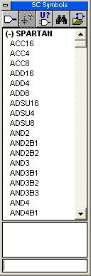
Use
Schematic Symbols window to select items for your circuit.
-
You can
type the name of the symbol or scroll down the list.
-
If your
item is not listed you can use the “Select Libraries” button to add more
symbols.
![]()
-
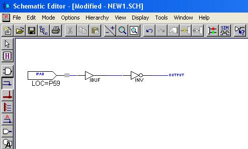
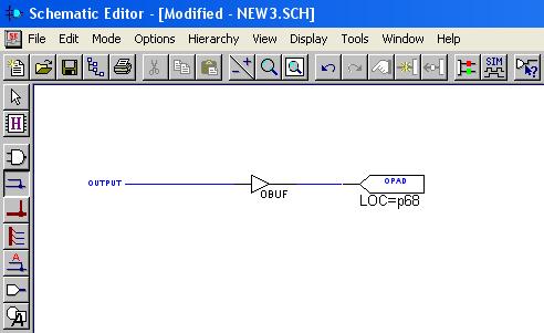
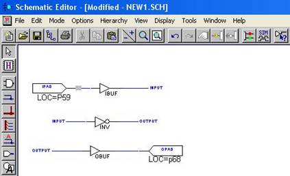
Every
Input is defined using IPAD and must be followed by IBUF
-
Every
Output is defined using OPAD and must be preceded by OBUF
-
Input(s)
& Output(s): Must be
assigned PIN LOCALIZATION NUMBERS.
i.
To input
pin localization, dbl-click IPAD or OPAD and you will see a panel that
shows the symbol properties. The Name
and Description Parameters will be used to enter the pin
specifications. THIS IS NECESSARY FOR
THE COMPILED SCHEMATIC TO DOWNLOAD CORRECTLY TO THE PROTOTYPING BOARD. ELSE AND ERROR SUCH AS “NODE NOT FOUND” WILL
APPEAR WHEN COMPILING.
j.
The following
shows how to make an input buffer a push button (P59 represents Push
button 1) on the board. Under Parameters, Name should always be LOC and Description
is the desired pin number (obtained from the table under section m).
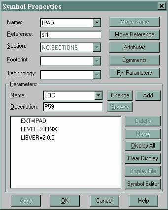
k. BE SURE TO CLICK ON THE ADD BUTTON!!!
You will see the pin localization added to the Description list. ![]()
l.
Any changes made to the Description after
adding occur as long as you click OK.
![]()
m. The pinout table
provided is online and available to anyone, but for our purposes, it will be
displayed in the following pages. The grayed pin numbers can not be used as
outputs. [2]:
|
Pin |
Connection |
Description |
|
1 |
GND |
Ground |
|
2 |
Vcc |
Power |
|
3 |
PWE |
Parallel port Write Enable (in EPP mode) |
|
4 |
PD0 |
Parallel port data pin 0 |
|
5 |
PD1 |
Parallel port data pin 1 |
|
6 |
PD2 |
Parallel port data pin 2 |
|
7 |
PD3 |
Parallel port data pin 3 |
|
8 |
PD4 |
Parallel port data pin 4 |
|
9 |
PAS |
Parallel port Address Strobe (in EPP mode) |
|
10 |
PRS |
Parallel port Reset (in EPP mode) |
|
11 |
Vcc |
Power |
|
12 |
GND |
Ground |
|
13 |
CLK1 |
External clock signal 1 (25.175MHz) |
|
14 |
PDS |
Parallel port Data Strobe (in EPP mode) |
|
15 |
PWT |
Parallel port Wait (in EPP mode) |
|
16 |
PD5 |
Parallel port data pin 5 |
|
17 |
PD7 |
Parallel port data pin 7 |
|
18 |
PD6 |
Parallel port data pin 6 |
|
19 |
SW8 |
Slide switch 8 |
|
20 |
SW7 |
Slide switch 7 |
|
21 |
GND |
Ground |
|
22 |
Vcc |
Power |
|
23 |
SW6 |
Slide switch 6 |
|
24 |
SW5 |
Slide switch 5 |
|
25 |
SW4 |
Slide switch 4 |
|
26 |
SW3 |
Slide switch 3 |
|
27 |
SW2 |
Slide switch 2 |
|
28 |
SW1 |
Slide switch 1 |
|
29 |
CG |
Seven-segment Cathode connection g |
|
30 |
M1_NC |
Mode pin 1 (not connected) |
|
31 |
GND |
Ground |
|
32 |
MODE |
Mode pin 0 |
|
33 |
Vcc |
Power |
|
34 |
M2_NC |
Mode pin 2 (not connected) |
|
35 |
CLK2 |
Clock 2 (not connected) |
|
36 |
|
Not connected |
|
37 |
|
Not connected |
|
38 |
A4 |
Anode of digit 4 |
|
39 |
A3 |
Anode of digit 3 |
|
40 |
A1 |
Anode of digit 2 |
|
41 |
INIT (O4) |
INIT pin. User-defined pin 4 |
|
42 |
Vcc |
Power |
|
43 |
GND |
Ground |
|
44 |
A2 |
Anode of digit 1 |
|
45 |
CG |
Cathode of segment G |
|
46 |
CF |
Cathode of segment F |
|
47 |
CE |
Cathode of segment E |
|
48 |
CD |
Cathode of segment D |
|
49 |
CC |
Cathode of segment C |
|
50 |
CB |
Cathode of segment B |
|
51 |
CA |
Cathode of segment A |
|
52 |
GND |
Ground |
|
53 |
DONE |
DONE signal pin |
|
54 |
Vcc |
Power |
|
55 |
PROGRAM |
PROGRAM signal pin |
|
56 |
BTN4 |
Push button 4 |
|
57 |
BTN3 |
Push button 3 |
|
58 |
BTN2 |
Push button 2 |
|
59 |
BTN1 |
Push button 1 |
|
60 |
LD8 |
LED 8 |
|
61 |
LD7 |
LED 7 |
|
62 |
LD6 |
LED 6 |
|
63 |
Vcc |
Power |
|
64 |
GND |
Ground |
|
65 |
LD5 |
LED 5 |
|
66 |
LD4 |
LED 4 |
|
67 |
LD3 |
LED 3 |
|
68 |
LD2 |
LED 2 |
|
69 |
LD1 |
LED 1 |
|
70 |
LDG |
Gate connection for LED driver |
|
71 |
DIN (O5) |
DIN pin. User-defined pin 5 |
|
72 |
RXD |
DOUT pin. Serial RS-232 receive pin |
|
73 |
CCLK |
Configuration clock |
|
74 |
Vcc |
Power |
|
75 |
TXD |
Serial RS-232 transmit pin |
|
76 |
GND |
Ground |
|
77 |
R |
VGA red signal pin |
|
78 |
G |
VGA green signal pin |
|
79 |
B |
VGA blue signal pin |
|
80 |
HS |
VGA horizontal sync pin |
|
81 |
VS |
VGA vertical sync pin |
|
82 |
PS2C |
PS2 Clock pin |
|
83 |
PS2D |
PS2 Data pin |
|
84 |
PINT |
Parallel port Interrupt |
n. Board Layout:
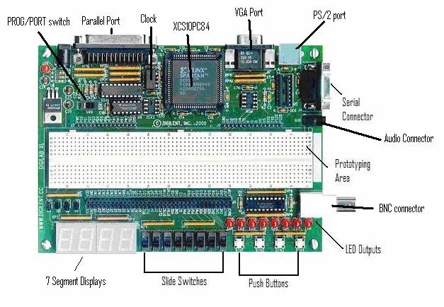
Note: Not
all of the inputs/outputs can be used in a design implementation. For example,
the PS/2 port requires components that are not on the board.
IV.
Design Using HDL
a. While our software license doesn’t allow HDL-created designs to be implemented, it does allow use of some other HDL development features.
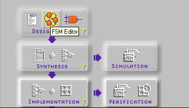
b. After creating an empty project, instead of clicking on the schematic editor, click on the FSM editor (Xilinx will ask for a new license file, click cancel for limited functionality):
c. Once in the FSM editor, states can be added by clicking on the state icon, and adding a state to the editing area:
d. After
states are added, transitions are added
to produce a FSM map: 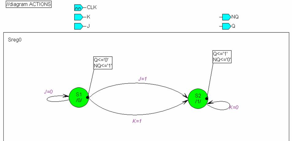
A FSM for a JK flip-flop
e. Once a FSM map has been input, Xilinx will generate HDL code corresponding to the FSM (in this case, in Verilog):
//
// File: U:\Public\HDLtest\JK.v
// created: 02/20/06 16:55:13
// from: 'U:\Public\HDLtest\JK.asf'
// by fsm2hdl - version: 2.0.1.60
//
module JK (CLK, J, K, NQ, Q);
input CLK;
input J;
input K;
output NQ;
output Q;
reg NQ;
reg Q;
// SYMBOLIC ENCODED state machine: Sreg0
parameter S1 = 1'b0,
S2 = 1'b1;
reg CurrState_Sreg0, NextState_Sreg0;
// Diagram actions (continuous assignments allowed only: assign ...)
//diagram ACTIONS;
// Machine: Sreg0
// NextState logic (combinatorial)
always @ (J or K or CurrState_Sreg0)
begin
case (CurrState_Sreg0)
S1:
begin
Q<='0'
NQ<='1';
if (K=1)
begin
NextState_Sreg0 = S2;
end
else if (J=0)
begin
NextState_Sreg0 = S1;
end
else if (J=1)
begin
NextState_Sreg0 = S2;
end
end
S2:
begin
Q<='1'
NQ<='0';
if (K=0)
begin
NextState_Sreg0 = S2;
end
end
endcase
end
// Current State Logic (sequential)
always @ (posedge CLK)
begin
CurrState_Sreg0 <= NextState_Sreg0;
end
endmodule
f. Additionally, HDL designs can be entered manually. The simulation, implementation, and programming steps are not available for HDL-based projects with our license.
V.
SIMULATION
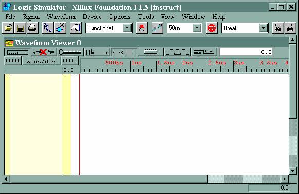
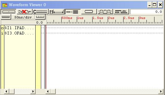
a. After verifying the schematic has all inputs,
outputs, and pinouts, you are ready to simulate. Click on the Simulator button ![]() in the main toolbar at the top of the editor
and you will see the following:
in the main toolbar at the top of the editor
and you will see the following:
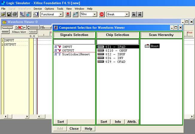
b.
Click on the Signal tab and Add Signals. The following window will appear:
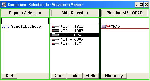
c.
Under Chip
Selection: Highlight an IPAD or OPAD
-
Note: Net
Names can be used instead of IPAD or OPAD (See Section VII: Special
Techniques)
d.
Double
click on the respective part which appears under the Pins for section. Repeat for each input and output. You
must select all push buttons and output devices, not the intermediate
components (e.g. flip flops, nand gates). This process adds each signal to the Waveform
Viewer as shown below.
e.
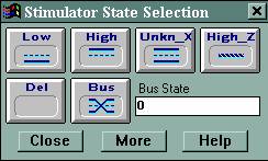
Once finished, highlight an input component then
click on the Logical States button ![]() which will bring up
this window:
which will bring up
this window:
f.
This will
allow the input to be initialized, to whichever starting state is
necessary. Most likely, you will select
the Low signal button.
g. Afterwards, you can switch through states
with the previous window, and execute the program through intervals of
microseconds (µs) per execution. To go
through a step of the execution, you must click on the Simulation Step
button ![]() .
.
h. Remember,
flip flops work with up switching and down switching which means you must go low_high_low if it’s an up switch and high_low_high
for down switching. That is the only way
to activate the component.
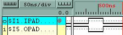
i.
The output should show up like a step function and
you can compare states using the simulation before downloading to the board:
j.
At any
point in the simulation, Xilinx will place markers on named nets that are added
signals indicating their state: Red for 1, Green for 0, and Blue for unknown:
k. Observing
the states on the schematic diagram can help with debugging.
VI.
IMPLEMENTATION
a. After the circuit
is simulated and working properly you can than proceed to implement your circuit on the
FPGA.
b. First make sure that the FPGA is properly
connected (parallel and power cables).
c. Next click on the Implementation button.
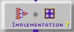
d. The Implementation process is automated. The Implementation window (shown below), will pop-up on its own and if there are no errors the status indicator will read “OK” upon the completion of this process.
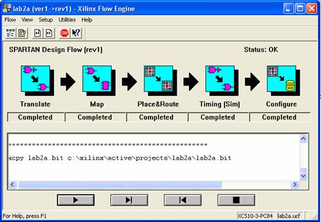
Common Errors:
Specified Revision is Invalid: The project needs to be reopened. Delete a directory if one is specified to be removed manually.
ERROR:NgdBuild:466 - input pad net '$Net00002_' has illegal connection: one of the input pads either doesn’t have a pin specified, is a duplicate of another input pads, or is not connected to an IBUF.
Having unconnected pins will only result in an error sometimes, even when it will result in a change to functionality.
Having floating pins can result in errors during implementation.
It is easy to mix up the LSB and MSB when using some functional blocks. Data sheets are available for each block online at http://toolbox.xilinx.com/docsan/xilinx5/data/docs/lib/lib0024_8.html. Note that some of these designs are not available for the Spartan FPGA that we use.
VII.
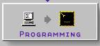
PROGRAMMING
a. The next step is to download the circuit into the FPGA. To accomplish this press the Programming button, select iMPACT and press OK.
b. In the iMPACT window
select the tab that says Slave Serial.
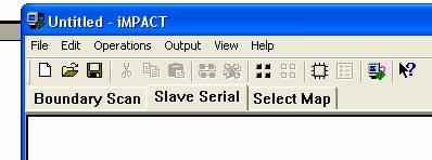
c. Right click in the white area and select Add
Xilinx Device. In the next window
that pops up select
the .bit file that corresponds to your project (ie. YourProjectName.bit).
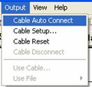
d. Next, select the Output menu and click
on Cable Auto Connect.
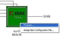
e. Than click on the image of the Xilinx chip so
that it is highlighted. Right click on
the image and click on
Program. If successful the words Programming
Succeeded should appear at the bottom of the screen.
f.
The FPGA
should now be programmed and ready for use. If the programming fails, check to
make sure the settings for the project are correct. In the project manager,
chose “Project Type…” and enter the correct configuration.
VIII.
Special
Techniques
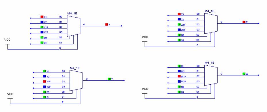
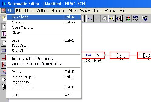
a. Net Names can be used to link logic
circuits across schematics thus organizing inputs and outputs. New Schematics
can be added by selecting New Sheet
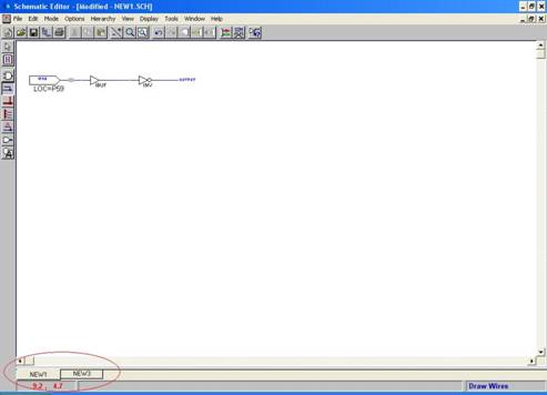
under the file menu in the Schematic Editor.
- Alternating between sheets can be performed by clicking on the corresponding tab at the bottom left corner of the Schematic Editor.
- Net Names can be connected to the
output of IBUF or the input of OBUF.
These names can then be used in the simulation in order to label
inputs and outputs clearly as demonstrated below:
- Upon selecting Add Signal under the signal menu, the component selection screen appears. Net names are added to the simulation, as signals, by double clicking on the respective name under the Signal Selection heading.
b. Quickly creating input signals:
Technique 1:
Highlight an input, and click on the stimulator selection symbol from the toolbar. Click on a letter from the keyboard window.
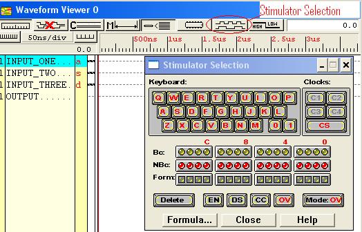
In this case, “INPUT” is assigned ‘a’. Whenever you press ‘a’ on the keyboard, the state of that symbol will change.
Technique 2:
You can assign clock pulses to each symbol called the waveform using formula.
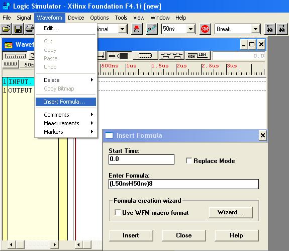
In the formula, (L50nsH50ns)8, ‘L’ is low and ‘H’ is high. ‘50ns’ is the time for which that signal (high or low) lasts. And ‘8’ is the number of times the pattern is to be repeated. By entering different formulas, every combination of inputs can be easily analyzed. For example, set one input to (L100nsH50ns) and another to (L50nsH50ns)2 to have every combination for two inputs.
SOURCES
[1]
J. Wunderlich. Advanced
Computer Engineering Class Notes.
[2]
“Original Digilab Pinouts”
[3] Image Processing
Applications On New Generation FPGAs
by Rahul V. Shah, eInfochips
Ltd. http://www.fpgajournal.com/articles_2006/20060307_einfo.htm
[4] Terminology Tango 101 http://www.fpgajournal.com/articles/20040706_tango.htm
“Spartan &
Spartan-XL FPGAs”
http://www.xilinx.com/products/silicon_solutions/fpgas/spartan_series/spartanxl_fpgas/index.htm
“Reconfigurable Computing
in Real-World Applications” by Steve Margerm, Senior
Hardware Designer, Cray, Inc. http://www.fpgajournal.com/articles_2006/20060207_cray.htm
“Field-programmable gate array” http://en.wikipedia.org/wiki/Fpga
“Digilab Board Description” by Jan
Van der Spiegel (2002)